




- sales/support
Google Chat:---
- sales
+86-0755-88291180
- sales01
sales@spotpear.com
- sales02
dragon_manager@163.com
- support
tech-support@spotpear.com
- CEO-Complaints
zhoujie@spotpear.com
- Only Tech-Support
WhatsApp:13246739196
- Purchase/Shipping/Refund
WhatsApp:13424403025
- HOME
- >
- ARTICLES
- >
- Common Moudle
- >
- UART Module
Modbus RTU Module (A) User Guide
Specifications
Communication Parameters
| Parameter | Specification |
|---|---|
| Supply Voltage | 7 V ~ 36 V |
| Communication Interface | RS485 |
| Baud Rate | 2400, 4800, 9600, 19200, 38400, 57600, 115200, 128000, 256000 |
| Default Communication Format | 9600, N, 8, 1 |
| Modbus Protocol | Standard Modbus RTU Protocol |
| RS485 Address Range | 1 ~ 255 |
| Indicator LEDs | STA: MCU status, flashes when MCU is working normally TXD: Transmit indicator, lights when sending data RXD: Receive indicator, lights when receiving data |
Input/Output Parameters
| Parameter | Specification |
|---|---|
| Relay Output | 2 DO, 1 normally open + 1 normally closed, ≤10 A 250 V AC or ≤10 A 30 V DC |
| Digital Input | 2 DI, 5 V ~ 36 V, dry contact / wet contact (NPN or PNP), built-in bidirectional optocoupler |
| Analog Output | 2 AO, 0 ~ 20 mA, 12-bit resolution, 1 μA, accuracy ±0.03 mA |
| Analog Input | 2 AI, 0 ~ 10 V / 2 ~ 10 V / 0 ~ 20 mA / 4 ~ 20 mA, 12-bit resolution, accuracy ≤3‰, update rate 31 Hz, sampling resistor 249 Ω |
Relay Output
| Parameter | Specification |
|---|---|
| Number of Relays | 2 |
| Contact Type | 1 normally open + 1 normally closed |
| Contact Load | ≤10 A 250 V AC or ≤10 A 30 V DC |
Analog Output
| Parameter | Specification |
|---|---|
| Output Mode | 2 current outputs |
| Resolution | 12 bits, 1 μA |
| Range | 0 ~ 20 mA |
| Output Accuracy | ±0.03 mA |
Digital Input
| Parameter | Specification |
|---|---|
| Number of Inputs | 2 |
| Wet Contact Range | 5 V ~ 36 V DC |
| Input Type | Dry contact / wet contact (NPN or PNP) |
| Isolation Type | Bidirectional optocoupler |
Analog Input
| Parameter | Specification |
|---|---|
| Number of Inputs | 2 |
| Range | 0 ~ 10 V / 2 ~ 10 V 0 ~ 20 mA / 4 ~ 20 mA |
| Sampling Accuracy | 12-bit resolution, accuracy ≤3‰ |
| Data Update Rate | 31 Hz |
| Current Sampling Resistor | 249 Ω |
Basic Functions
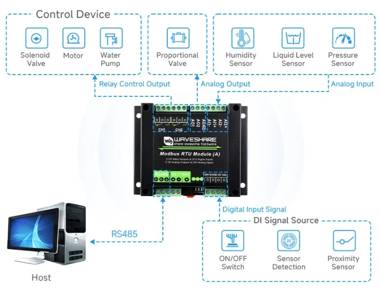
Supports digital and analog input/output via RS485 sending Modbus RTU protocol commands.
Hardware Description
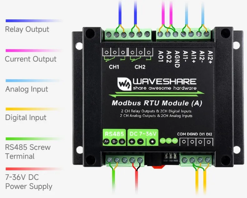
Hardware Terminal Description
Product Wiring Table
Relay Output
| Terminal Label | Function |
|---|---|
| CH1 NC | Relay CH1 normally closed contact |
| CH1 COM | Relay CH1 common terminal |
| CH1 NO | Relay CH1 normally open contact |
| CH2 NC | Relay CH2 normally closed contact |
| CH2 COM | Relay CH2 common terminal |
| CH2 NO | Relay CH2 normally open contact |
Analog Input/Output
| Terminal Label | Function |
|---|---|
| AO1 | Analog output channel 1 |
| AO2 | Analog output channel 2 |
| AGND | Analog ground |
| AI1+ | Analog input channel 1 positive terminal |
| AI1- | Analog input channel 1 negative terminal |
| AI2+ | Analog input channel 2 positive terminal |
| AI2- | Analog input channel 2 negative terminal |
Communication and Power Supply
| Terminal Label | Function |
|---|---|
| 485 A+ | RS485 signal line A+ |
| 485 B- | RS485 signal line B- |
| EARTH | RS485 shield ground |
| DC 7 ~ 36 V + | Power supply positive |
| DC 7 ~ 36 V - | Power supply negative |
| ⊙ DC 7 ~ 36 V | Round DC power connector |
The round DC power connector and the screw terminal power input must not be connected simultaneously. Doing so may damage the power supply or the module, or cause other safety risks.
Digital Input
| Terminal Label | Function |
|---|---|
| DI COM | Digital input common terminal |
| DGND | Digital ground |
| DI1 | Digital input channel 1 |
| DI2 | Digital input channel 2 |
DI COM Terminal
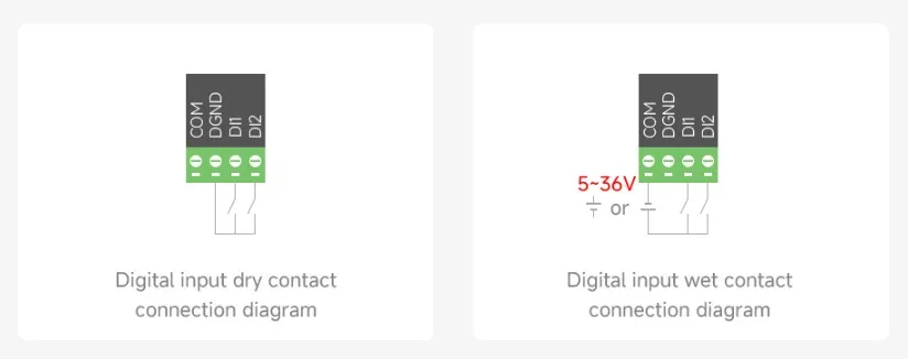
↑ DI COM is the common terminal for input signals. It can be left unconnected, connected to power positive, or power negative. It can be powered directly from the supply voltage or from an independent power source.
Three connection methods:
- Unconnected (floating): dry contact input
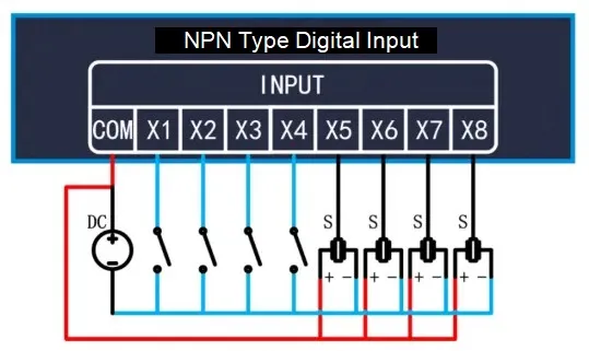
- Connected to power positive: active low trigger, NPN-type wet contact input, voltage 5V-36V DC
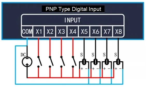
- Connected to power negative: active high trigger, PNP-type wet contact input, voltage 5V-36V DC
Digital Input Wiring
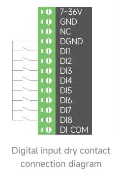
The digital input wiring types: passive dry contact input, active wet contact NPN input, active wet contact PNP input.
Dry Contact Input Wiring Diagram
Active Wet Contact NPN Input Wiring Diagram
Active Wet Contact PNP Input Wiring Diagram
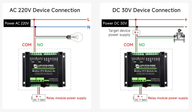
Relay Output Wiring
Normally Open Relay Output Wiring Diagram
Connect the live wire (for AC loads) or power positive (for DC loads) to the COM terminal, then connect from the normally open (NO) terminal to the load.
Analog Input Wiring
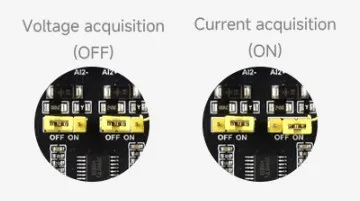
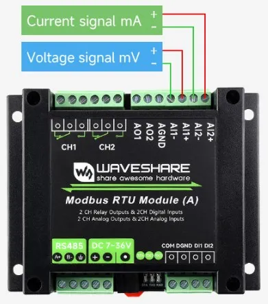
When opening the device enclosure, you will find jumpers near the device terminals, corresponding to channels AI1~AI2. The jumper mode must be selected according to the measured signal, otherwise measurement data will be inaccurate.
- For voltage signal measurement, disconnect the jumper for the corresponding channel.
- For current signal measurement, connect (short) the jumper for the corresponding channel.
AI+ is the positive input terminal, AI- is the negative input terminal.
For current measurement, current flows into AI+ and out of AI-; for voltage measurement, connect voltage positive to AI+ and voltage negative to AI-.
Current Output Wiring
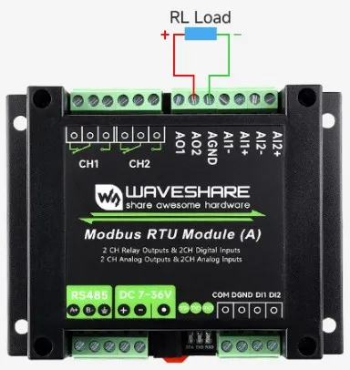
Connect AO to the load positive terminal and AGND to the load negative terminal.
Power and Communication Connection
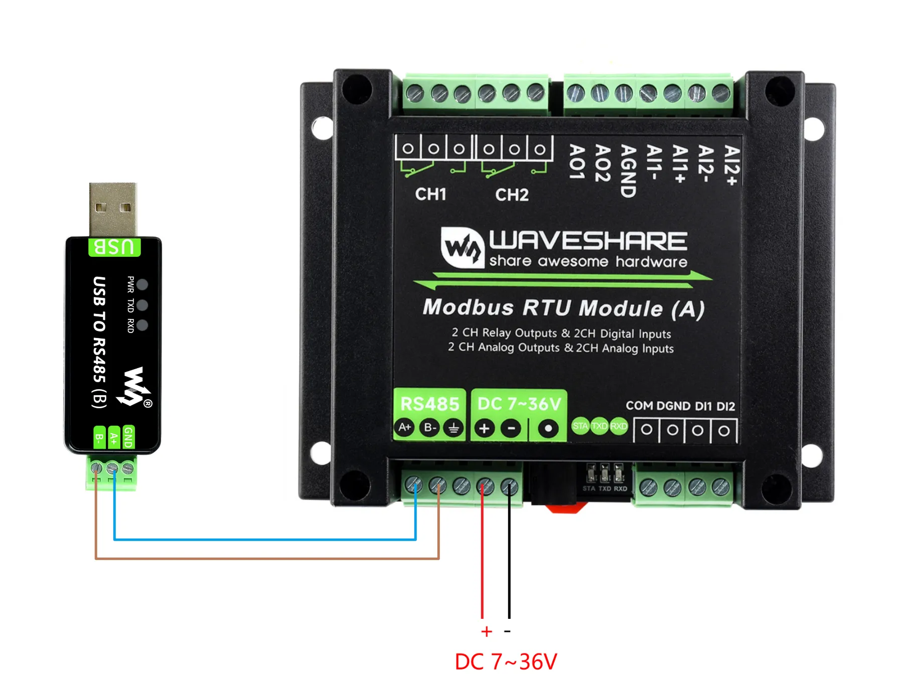
Connect the USB TO 485 converter to the target board using jumper wires, connecting A-->A and B-->B as shown in the figure below:
Software Test
The demonstration introduces the operation methods of the following two software tools. The SSCOM serial port debugging assistant is more convenient to operate, requires no installation, and displays complete commands for easier analysis. The disadvantage is that the data is not intuitive. The Modbus Poll software operates directly on registers, making data observation more intuitive. Its disadvantage is that it does not display full commands, requiring familiarity with Modbus register operations.
You can choose either method for testing. It is recommended to use the SSCOM Serial Port Debug Assistant for the first test.
SSCOM Serial Port Debugging Assistant
Download SSCOM Serial Debugging Assistant and open it on your computer. Select the correct COM port, set baud rate to 9600, select HEX send and receive, enable Modbus CRC16 check, click "Multi_Strings" to open the send multi char window, and then click the corresponding function button to send the corresponding command.
- Turn on channel 1 relay
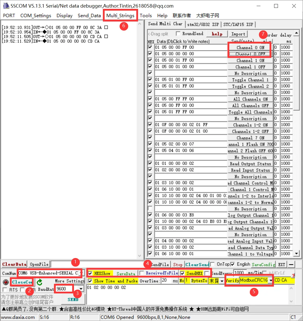
NOTEThe module defaults to Normal mode upon delivery, and relays can be controlled directly via commands. If a command returns normally but the relay does not act, the module may have been switched to another control mode. You can check this by reading the Relay Control Mode command.
- Turn on channel 1 relay
To send other commands, select SendHEX, enable Modbus CRC16 check, enter the first six bytes of the command, and click Send. The software will automatically append the CRC code. For example, send the following command to set analog channel 1 to output 1 mA:
01 06 00 00 03 E8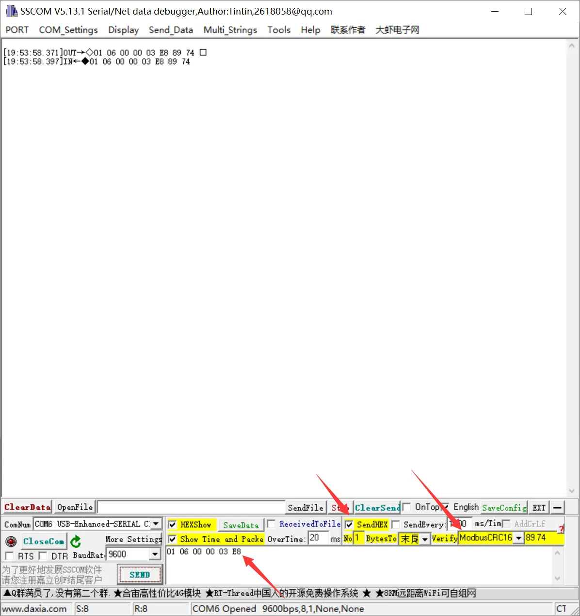
For more detailed control commands, please refer to the Development Protocol.
Modbus Poll Software
Relay Output
If the serial port software is inconvenient for observing data, you can choose the Modbus Poll software to read data. Download and install the Modbus Poll software.
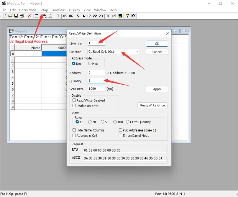
Open the software, select Setup -> Read/Write Definition. Set Slave ID to the actual device address, Function to 01 Read Coils, Quantity to 2 channels. Click OK to confirm.
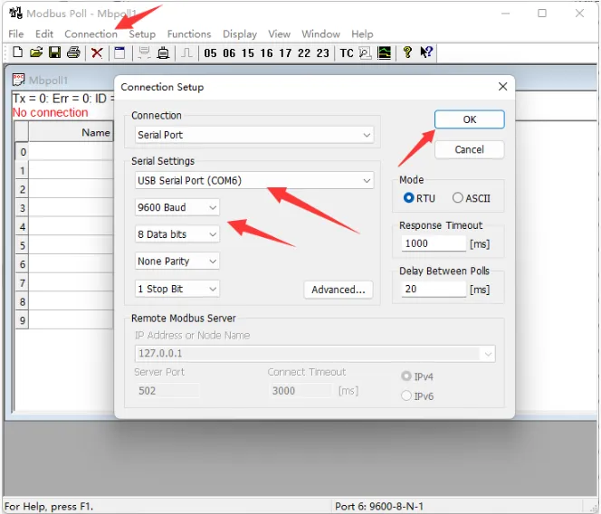
Select Connection->Connect..., choose the corresponding serial port, set the baud rate to 9600, and select 8 Data bits and None Parity. Click OK to connect.
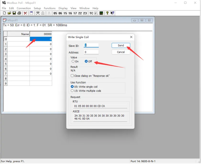
Once connected, you can view the current output channel status. Select the desired channel, double-click the status value to open the send dialog, choose On or Off, then click Send to control the relay.
Digital Input
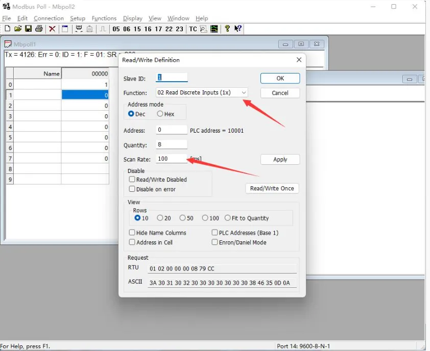
Select File -> New to create a new window. Select Setup -> Read/Write Definition. Set Slave ID to the actual device address, Function to 02 Read Discrete Inputs, Address to 0, Quantity to 2 channels, Scan Rate to 100 ms. Click OK to confirm.
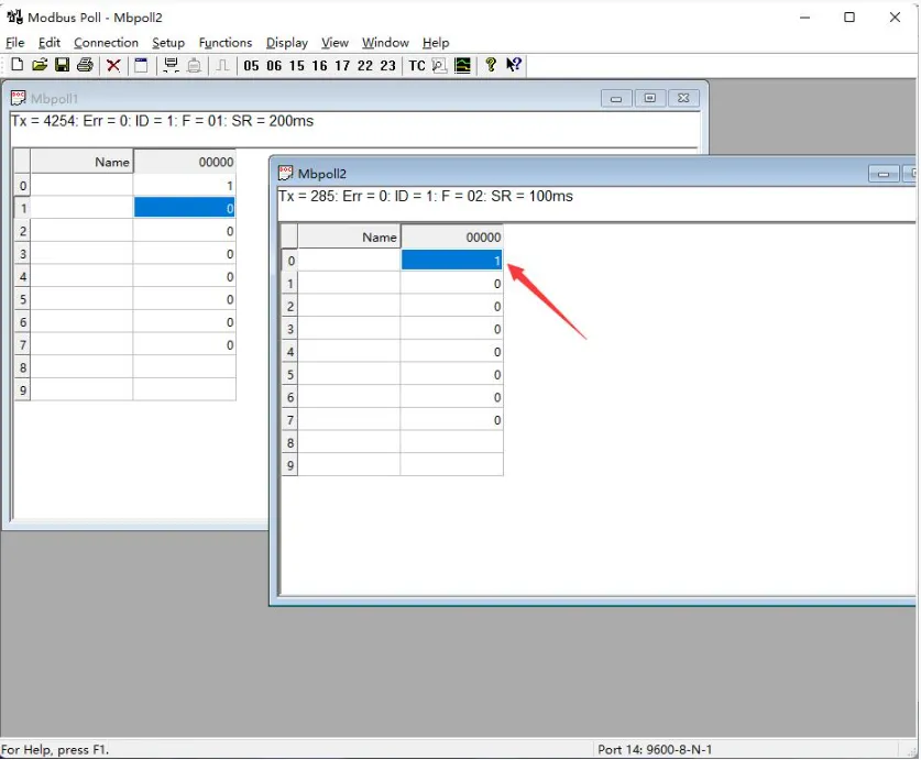
The newly created window 2 can display the current input status. Changing the input interface level will also change the corresponding value.
 RECOMMENDATION
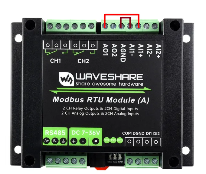
The following tests use AO1 and AI2 as examples. To achieve the same test results, complete the wiring first, then set the current output parameters. Do not enable current output before wiring is complete.
Current Output
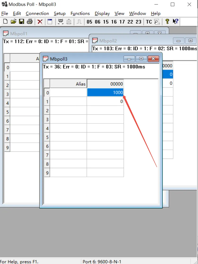
Select File -> New to create a new window. Select Setup -> Read/Write Definition. Set Slave ID to the actual device address, Function to 03 Read Holding Registers, Address to 0, Quantity to 2 channels, Scan Rate to 100 ms. Click OK to confirm.
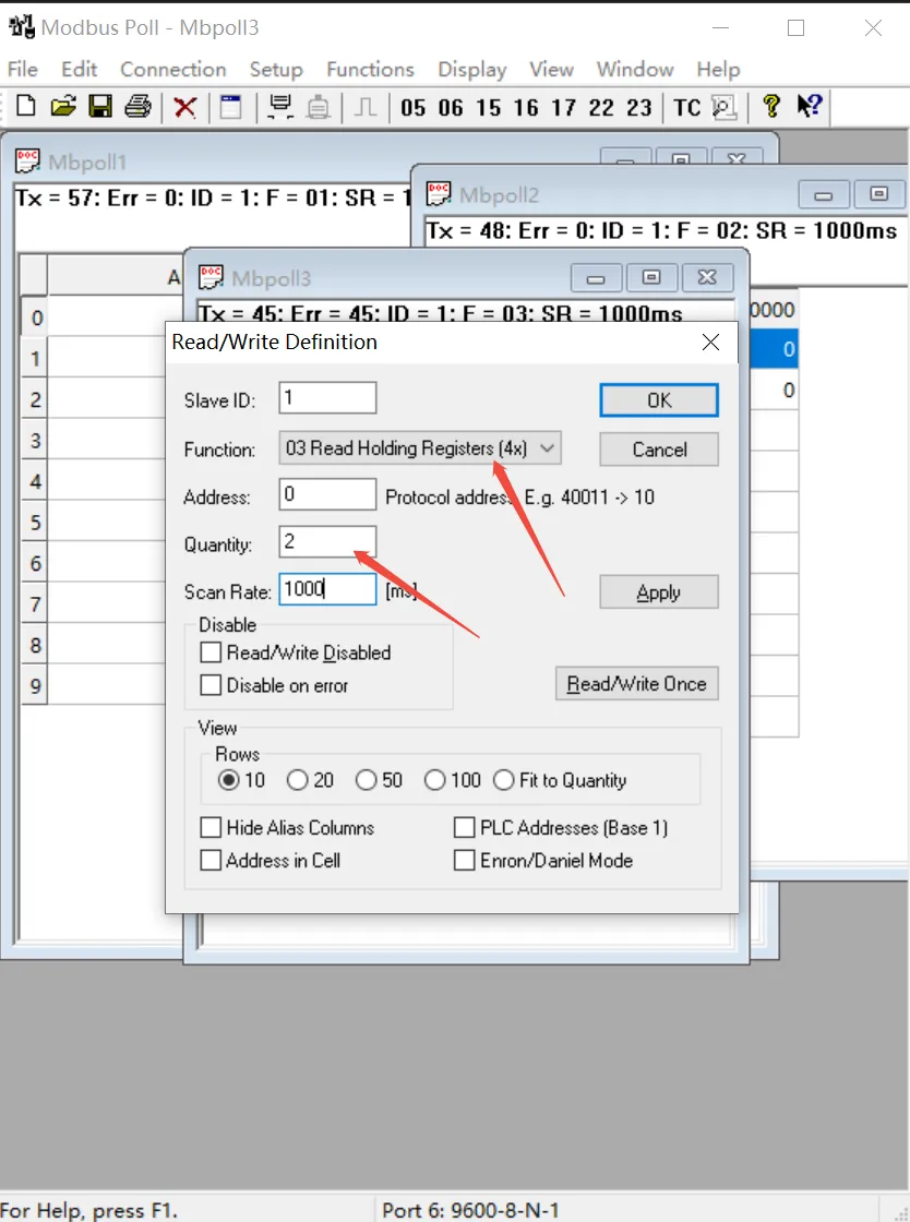
The new window (window 3) will display the register values for the current output channels. Adjusting the output current will change the corresponding register values.
Analog Input Channel Data Type
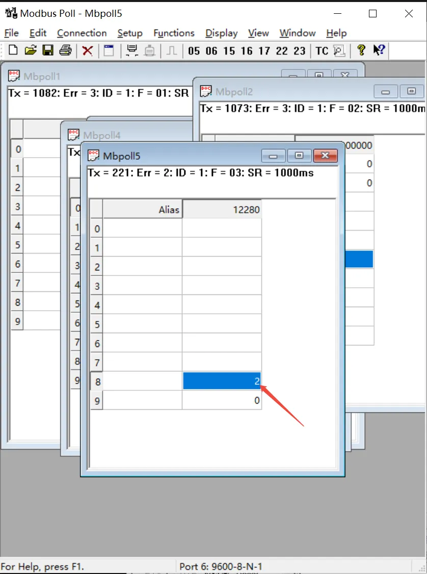
Select File -> New to create a new window. Select Setup -> Read/Write Definition. Set Slave ID to the actual device address, Function to 03 Read Holding Registers, Address to 12288, Quantity to 2 channels, Scan Rate to 100 ms. Click OK to confirm.
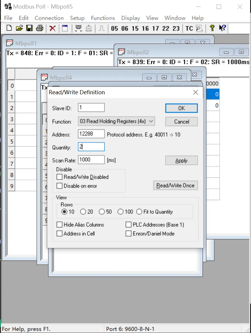
The new window (window 4) will display the data type of the analog input channels. After changing an analog input channel's data type to 02 (0 ~ 20 mA range), the corresponding register value will change.
Analog Input
Select File -> New to create a new window. Select Setup -> Read/Write Definition. Set Slave ID to the actual device address, Function to 04 Read Input Registers, Address to 0, Quantity to 2 channels, Scan Rate to 100 ms. Click OK to confirm.
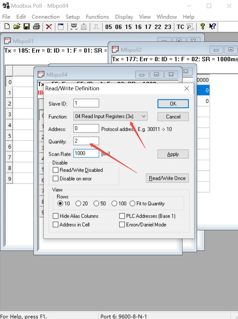
The new window (window 5) will display the sampled values of the analog input channels. Adjusting the output channel current will cause the input channel's measured current to change, and the corresponding register values will update accordingly.
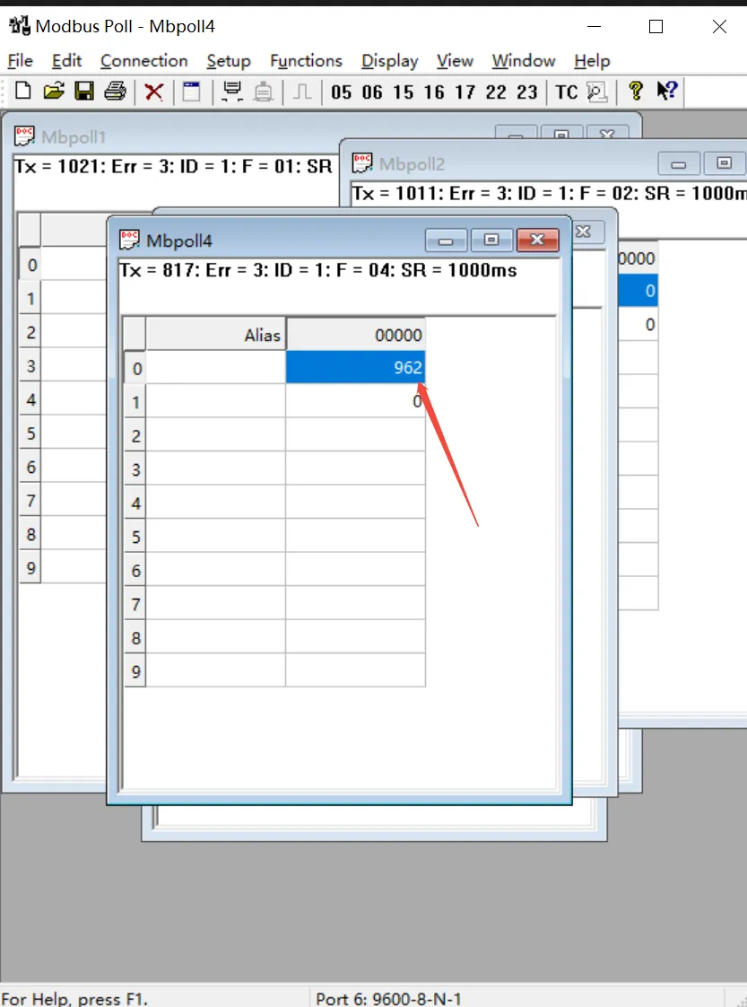
Result Explanation: Output channel accuracy is ±0.03 mA. Due to output cable loss and analog acquisition accuracy errors, the actual read register values may deviate slightly. Therefore, measurement results around 960 are within the normal range.
Development Protocol
Function Code Introduction
| Function Code | Description |
|---|---|
| 01 | Read Output Status |
| 02 | Read Input Status |
| 03 | Read Holding Registers |
| 05 | Write Single Output Channel |
| 06 | Write Single Register |
| 0F | Write Multiple Output Channels |
| 10 | Write Multiple Registers |
Register Address Description
| Address (HEX) | Content Stored | Register Value | Access | Modbus Function Code |
|---|---|---|---|---|
| 0x0000 - 0x0001 | Output Channel 1 - Output Channel 2 Address | 0xFF00: ON; 0x0000: OFF; 0x5500: Toggle | R/W | 0x01, 0x05, 0x0F |
| 0x00FF | Operate All Registers | 0xFF00: All Output ON; 0x0000: All Output OFF; 0x5500: All Output Toggle | W | 0x05, 0x0F |
| 0x0100 - 0x0101 | Output Channel 1 - Output Channel 2 Address | 0xFF00: Toggle; 0x0000: No Change | W | 0x05 |
| 0x0200 - 0x0201 | Output Channel 1 - Output Channel 2 Flash ON | Delay time = data × 100 ms Value: 0x0007, delay: 7 × 100 ms = 700 ms | W | 0x05 |
| 0x0400 - 0x0401 | Output Channel 1 - Output Channel 2 Flash OFF | Delay time = data × 100 ms Value: 0x0007, delay: 7 × 100 ms = 700 ms | W | 0x05 |
| 1x0000 - 1x0001 | Input Channel 1 - Input Channel 2 Address | Status of input channels 1-2 | R | 0x02 |
| 3x0000 - 3x0001 | Analog Input Channel 1 - Analog Input Channel 2 Data | Unsigned hexadecimal value | R | 0x04 |
| 4x0000 - 4x0001 | Analog Output Channel 1 - Analog Output Channel 2 Data | Unsigned hexadecimal value | R/W | 0x03, 0x06, 0x10 |
| 4x1000 - 4x1001 | Output Channel 1 - Output Channel 2 Control Mode | 0x0000-0x0003 Four control modes | R/W | 0x03, 0x06, 0x10 |
| 4x3000 - 4x3001 | Analog Input Channel 1 - Analog Input Channel 2 Data Type | 0x0000-0x0004 Five ranges | R/W | 0x03, 0x06, 0x10 |
| 4x2000 | Serial Parameters | High byte: parity (0x00-0x02) Low byte: baud rate (0x00-0x07) | R/W | 0x03, 0x06 |
| 4x4000 | Device Address | Directly stores Modbus address Device address: 0x0001-0x00FF | R/W | 0x03, 0x06 |
| 4x8000 | Software Version | Convert to decimal and shift decimal point left two places 0x0064 = 100 = V1.00 | R | 0x03 |
Modbus RTU Digital Channel Commands
Control a Single Output Channel
Transmission Code: 01 05 00 00 FF 00 8C 3A
| Field | Description | Notes |
|---|---|---|
| 01 | Device Address | 0x00: broadcast; 0x01-0xFF: device address |
| 05 | Command 05 | Write single output channel |
| 00 00 | Address | Register address of output channel to control, 0x0000-0x0001 |
| FF 00 | Command | 0xFF00: ON; 0x0000: OFF; 0x5500: Toggle |
| 8C 3A | CRC16 | CRC16 checksum of the first 6 bytes of data |
Return Code: 01 05 00 00 FF 00 8C 3A
| Field | Description | Notes |
|---|---|---|
| 01 | Device Address | 0x00: broadcast; 0x01-0xFF: device address |
| 05 | Command 05 | Write single output channel |
| 00 00 | Address | Register address of output channel to control, 0x0000-0x0001 |
| FF 00 | Command | 0xFF00: ON; 0x0000: OFF; 0x5500: Toggle |
| 8C 3A | CRC16 | CRC16 checksum of the first 6 bytes of data |
Example: Device with address 1
Output channel 0 ON : 01 05 00 00 FF 00 8C 3A
Output channel 0 OFF : 01 05 00 00 00 00 CD CA
Output channel 1 ON : 01 05 00 01 FF 00 DD FA
Output channel 1 OFF : 01 05 00 01 00 00 9C 0A
Control All Relay Output Channels
Transmission Code: 01 05 00 FF FF 00 BC 0A
| Field | Description | Notes |
|---|---|---|
| 01 | Device Address | 0x00: broadcast; 0x01-0xFF: device address |
| 05 | Command 05 | Write single output channel |
| 00 FF | Address | Fixed 0x00FF |
| FF 00 | Command | 0xFF00: ON; 0x0000: OFF; 0x5500: Toggle |
| BC 0A | CRC16 | CRC16 checksum of the first 6 bytes of data |
Return Code: 01 05 00 FF FF 00 BC 0A
| Field | Description | Notes |
|---|---|---|
| 01 | Device Address | 0x00: broadcast; 0x01-0xFF: device address |
| 05 | Command 05 | Write single output channel |
| 00 FF | Address | Fixed 0x00FF |
| FF 00 | Command | 0xFF00: ON; 0x0000: OFF; 0x5500: Toggle |
| BC 0A | CRC16 | CRC16 checksum of the first 6 bytes of data |
Example: Device with address 1
All output channels ON : 01 05 00 FF FF 00 BC 0A
All output channels OFF : 01 05 00 FF 00 00 FD FA
All output channels TOGGLE: 01 05 00 FF 55 00 C2 AA
Read Relay Output Channel Status
Transmission Code: 01 01 00 00 00 02 BD CB
| Field | Description | Notes |
|---|---|---|
| 01 | Device Address | 0x00: broadcast; 0x01-0xFF: device address |
| 01 | Command 01 | Query output channel status |
| 00 00 | Output start address | Register address of output channel, 0x0000-0x0001 |
| 00 08 | Number of output channels | Number of output channels to read, cannot exceed max |
| 3D CC | CRC16 | CRC16 checksum of the first 6 bytes of data |
Return Code: 01 01 01 00 51 88
| Field | Description | Notes |
|---|---|---|
| 01 | Device Address | 0x00: broadcast; 0x01-0xFF: device address |
| 01 | Command 01 | Query output channel status |
| 00 00 | Output start address | Register address of output channel, 0x0000-0x0001 |
| 00 08 | Number of output channels | Number of output channels to read, cannot exceed max |
| 3D CC | CRC16 | CRC16 checksum of the first 6 bytes of data |
Example: Device with address 1
Transmit: 01 01 00 00 00 02 BD CB
Receive: 01 01 01 00 51 88    // All output channel OFF
Transmit: 01 01 00 00 00 02 BD CB
Receive: 01 01 01 01 90 48    // Output channel 0 ON, others OFF
Write Relay Output Channel Status
Transmission Code: 01 0F 00 00 00 02 01 03 9E 96
| Field | Description | Notes |
|---|---|---|
| 01 | Device Address | 0x00: broadcast; 0x01-0xFF: device address |
| 0F | Command 0F | Write output channel status |
| 00 00 | Output start address | Register address of output channel to control, 0x0000-0x0001 |
| 00 08 | Number of output channels | Number of output channels to operate, cannot exceed max |
| 01 | Byte count | Number of status bytes |
| 03 | Output status | Bit0: start output channel; Bit1: next output channel; high bits zero if idle |
| 9E 96 | CRC16 | CRC16 checksum of the first 6 bytes of data |
Return Code: 01 0F 00 00 00 02 D4 0A
| Field | Description | Notes |
|---|---|---|
| 01 | Device Address | 0x00: broadcast; 0x01-0xFF: device address |
| 0F | Command 0F | Write multiple relay status command |
| 00 00 | Output address | Register address of output channel, 0x0000-0x0007 |
| 00 02 | Number of outputs | Number of output channels operated |
| D4 0A | CRC16 | CRC16 checksum of the first 6 bytes of data |
Example: Device with address 1
All output channels ON : 01 0F 00 00 00 02 01 FF 9E D7
All output channels OFF : 01 0F 00 00 00 02 01 00 DE 97
Channel 0 ON; Channel 1 OFF: 01 0F 00 00 00 02 01 01 1F 57
Relay Output Channel Flash ON/OFF Commands
Transmission Code: 01 05 02 00 00 07 8D B0
| Field | Description | Notes |
|---|---|---|
| 01 | Device Address | 0x00: broadcast; 0x01-0xFF: device address |
| 05 | Command 05 | Single control command |
| 02 | Sub-command | 02 = Flash ON, 04 = Flash OFF |
| 00 | Output channel address | Output channel address, 0x00-0x07 |
| 00 07 | Interval time | Delay time = data × 100 ms Value: 0x0007, delay: 7 × 100 ms = 700 ms Max flash ON/OFF time 0x7FFF |
| 8D B0 | CRC16 | CRC16 checksum of the first 6 bytes of data |
Return Code: 01 05 02 00 00 07 8D B0
| Field | Description | Notes |
|---|---|---|
| 01 | Device Address | 0x00: broadcast; 0x01-0xFF: device address |
| 05 | Command 05 | Single control command |
| 02 | Sub-command | 02 = Flash ON, 04 = Flash OFF |
| 00 | Output channel address | Output channel address, 0x00-0x07 |
| 00 07 | Interval time | Delay time = data × 100 ms Value: 0x0007, delay: 7 × 100 ms = 700 ms Max flash ON/OFF time 0x7FFF |
| 8D B0 | CRC16 | CRC16 checksum of the first 6 bytes of data |
Example: Device with address 1
Output channel 0 flash ON: 01 05 02 00 00 07 8D B0  //700MS = 7*100MS = 700MS
Output channel 1 flash ON: 01 05 02 01 00 08 9C 74  //800MS
Output channel 0 flash OFF: 01 05 04 00 00 05 0C F9  //500MS
Output channel 1 flash OFF: 01 05 04 01 00 06 1D 38  //600MS
Read Digital Input Channel Status
Transmission Code: 01 02 00 00 00 02 F9 CB
| Field | Description | Notes |
|---|---|---|
| 01 | Device Address | 0x00: broadcast; 0x01-0xFF: device address |
| 02 | Command 02 | Read input status command |
| 00 00 | Input start address | Input register address, 0x0000-0x0001 |
| 00 02 | Number of registers | Number of input channels to read, cannot exceed max |
| F9 CB | CRC16 | CRC16 checksum of the first 6 bytes |
Return Code: 01 02 01 00 A1 88
| Field | Description | Notes |
|---|---|---|
| 01 | Device Address | 0x00: broadcast; 0x01-0xFF: device address |
| 02 | Command 02 | Read input status command |
| 01 | Byte count | Total number of bytes in the status information |
| 00 | Query status | Input channel status: Bit0 = start input channel, Bit1= next channel status, etc. high bits zero if idle |
| A1 88 | CRC16 | CRC16 checksum of the first 6 bytes of data |
Example: Device with address 1
Transmit: 01 02 00 00 00 02 F9 CB
Return: 01 02 01 00 A1 88    //Inputs are all untriggered
Transmit: 01 02 00 00 00 02 F9 CB
Return: 01 02 01 01 60 48    //Channel 1 input is triggered, and the rest of channels are not triggered
Read Relay Output Channel Control Mode
Transmit: 01 03 10 00 00 02 C0 CB
| Field | Description | Notes |
|---|---|---|
| 01 | Device Address | 0x00 indicates broadcast address; 0x01-0xFF indicate device address |
| 03 | 03 Command | Read Holding Registers |
| 10 00 | Register start address | 0x1000-0x1007 corresponds to output channels 1-8 |
| 00 02 | Number of registers | Number of registers to read, maximum 8 channels |
| C0 CB | CRC16 | CRC16 checksum of the first 6 bytes |
Return code: 01 03 04 00 00 00 00 FA 33
| Field | Description | Notes |
|---|---|---|
| 01 | Device Address | 0x00: broadcast; 0x01-0xFF: device address |
| 03 | Command 03 | Read holding registers |
| 04 | Byte count | Total number of bytes in the status information |
| 00 00 ...... 00 00 | Control mode | Control mode for output channels 1-2, 0x0000-0x0003 indicate four control modes: 0x0000: Normal mode – output controlled directly by command; 0x0001: Linkage mode – output follows corresponding input; 0x0002: Toggle mode – output toggles on each input pulse; 0x0003: Edge Trigger Mode – output toggles on each input level change |
| FA 33 | CRC16 | CRC16 checksum of the first 6 bytes |
Except for Link mode, all other modes also support command control of output channels.
Example: Device with address 1
Read output channel 1 control mode : 01 03 10 00 00 01 80 CA
Read output channel 2 control mode : 01 03 10 01 00 01 D1 0A
Set Single Output Channel Control Mode
Transmission Code: 01 06 10 00 00 01 4C CA
| Field | Description | Notes |
|---|---|---|
| 01 | Device Address | 0x00: broadcast; 0x01-0xFF: device address |
| 06 | Command 06 | Write single register command |
| 10 00 | Register start address | 0x1000-0x1007 corresponds to output channels 1-8 control mode |
| 00 01 | Control mode | Control modes for output channels 1-8, 4 control modes (0x0000-0x0003): 0x0000: Normal mode – output controlled directly by command; 0x0001: Linkage mode – output follows corresponding input; 0x0002: Toggle mode – output toggles on each input pulse; 0x0003: Edge Trigger Mode – output toggles on each input level change |
| 4C CA | CRC16 | CRC16 checksum of the first 6 bytes of data |
Except for Linkage mode, all other modes also support command control of output channels.
Return Code: 01 06 10 00 00 01 4C CA
| Field | Description | Notes |
|---|---|---|
| 01 | Device Address | 0x00: broadcast; 0x01-0xFF: device address |
| 06 | Command 06 | Write single register command |
| 10 00 | Register start address | 0x1000-0x1001 corresponds to output channels 1-2 control mode |
| 00 01 | Control mode | Output channel control modes, 0x0000-0x0003 indicate four control modes |
| 4C CA | CRC16 | CRC16 checksum of the first 6 bytes of data |
Example: Device with address 1
Set output channel 1 to Linkage mode: 01 06 10 00 00 01 4C CA
Set output channel 2 to Toggle mode: 01 06 10 01 00 02 5D 0B
Set Multiple Output Channel Control Modes
Transmit: 01 10 10 00 00 02 04 00 01 00 01 AE 6F
| Field | Description | Notes |
|---|---|---|
| 01 | Device Address | 0x00: broadcast; 0x01-0xFF: device address |
| 10 | Write Multiple Registers Command | |
| 10 00 | Register start address | 0x1000-0x1001 corresponds to output channels 1-2 control mode |
| 00 02 | Number of registers | Number of registers to set, up to 2 channels |
| 04 | Byte Count | Number of output bytes |
| 00 01 ...... 00 01 | Control mode | Control mode for output channels 1-2, 0x0000-0x0003 indicate four control modes: 0x0000: Normal mode – output controlled directly by command; 0x0001: Linkage mode – output follows corresponding input; 0x0002: Toggle mode – output toggles on each input pulse; 0x0003: Edge Trigger Mode – output toggles on each input level change |
| AE 6F | CRC16 | CRC16 checksum of the first 6 bytes |
Except for Linkage mode, all other modes also support command control of output channels.
Return Code: 01 10 10 00 00 02 45 08
| Field | Description | Notes |
|---|---|---|
| 01 | Device Address | 0x00: broadcast; 0x01-0xFF: device address |
| 10 | Write Multiple Registers Command | |
| 10 00 | Register start address | 0x1000-0x1007 corresponds to output channels 1-8 control mode |
| 00 02 | Number of registers | Number of registers to set, up to 8 channels |
| 45 08 | CRC16 | CRC16 checksum of the first 6 bytes of data |
Example: Device with address 1
Set channels 1-2 output as Linkage mode: 01 10 10 00 00 02 04 00 01 00 01 AE 6F
Set channels 1-2 output as Normal mode: 01 10 10 00 00 02 04 00 00 00 00 3E 6F
Modbus RTU Analog Channel Commands
Set Single Analog Output Channel
Send code: 01 06 00 00 03 E8 89 74
| Field | Description | Notes |
|---|---|---|
| 01 | Device Address | 0x00: broadcast; 0x01-0xFF: device address |
| 06 | Command 06 | Write single register command |
| 00 00 | Register address | 0x0000-0x0007 corresponds to output channels 1-8 |
| 03 E8 | Set Value | Hex value, unit μA, high byte first 0x03E8 = 1000 μA = 1 mA |
| 89 74 | CRC16 | CRC16 checksum of the first 6 bytes of data |
Return Code: 01 06 00 00 03 E8 89 74
| Field | Description | Notes |
|---|---|---|
| 01 | Device Address | 0x00: broadcast; 0x01-0xFF: device address |
| 06 | Command 06 | Write single register command |
| 00 00 | Register address | 0x0000-0x0007 corresponds to output channels 1-8 |
| 03 E8 | Set Value | Hex value, unit μA, high byte first 0x03E8 = 1000 μA = 1 mA |
| 89 74 | CRC16 | CRC16 checksum of the first 6 bytes of data |
Example: Device with address 1
Set channel 1 output 1mA : 01 06 00 00 03 E8 89 74
Set channel 2 output 5mA : 01 06 00 01 13 88 D5 5C
Set Multiple Analog Output Channels
Transmit: 01 10 00 00 00 02 04 03 E8 03 E8 73 61
| Field | Description | Notes |
|---|---|---|
| 01 | Device Address | 0x00: broadcast; 0x01-0xFF: device address |
| 10 | Write Multiple Registers Command | |
| 00 00 | Register Start Address | 0x0000 - 0x0002 correspond to output channels 1-2 |
| 00 02 | Number of Registers | Number of registers set, cannot exceed maximum channel count |
| 04 | Byte Count | Number of output bytes |
| 03 E8 ...... 03 E8 | Values | Start channel analog output …… Final channel analog output Hex, μA, high byte first, 0x03E8 = 1000 μA = 1 mA |
| 73 61 | CRC16 | CRC16 checksum of the first 6 bytes of data |
Return Code: 01 10 00 00 00 02 41 C8
| Field | Description | Notes |
|---|---|---|
| 01 | Device Address | 0x00: broadcast; 0x01-0xFF: device address |
| 10 | Write Multiple Registers Command | |
| 00 00 | Register start address | 0x0000-0x0007 corresponds to output channels 1-8 |
| 00 02 | Number of Registers | Number of registers set, cannot exceed maximum channel count |
| 41 C8 | CRC16 | CRC16 checksum of the first 6 bytes of data |
Example: Device with address 1
Set channels 1-2 output 1mA : 01 10 00 00 00 02 04 03 E8 03 E8 73 61
Set channels 1-2 output 2mA : 01 10 00 00 00 02 04 07 D0 07 D0 F0 8E
Read Analog Output
Transmit: 01 03 00 00 00 02 C4 0B
| Field | Description | Notes |
|---|---|---|
| 01 | Device Address | 0x00: broadcast; 0x01-0xFF: device address |
| 03 | Command 03 | Read holding registers |
| 00 00 | Starting register address | 0x0000 - 0x0001 correspond to relay control mode for channels 1-2 |
| 00 02 | Number of registers | Number of registers to read, cannot exceed maximum channel count |
| C4 0B | CRC16 | CRC16 checksum of the first 6 bytes of data |
Return Code: 01 03 04 03 E8 03 E8 7A FD
| Field | Description | Notes |
|---|---|---|
| 01 | Device Address | 0x00: broadcast; 0x01-0xFF: device address |
| 03 | Command 03 | Read holding registers |
| 04 | Byte count | Total number of bytes in the status information |
| 03 E8 ...... 03 E8 | Output values | Start channel analog output …… Final channel analog output Hex, μA, high byte first, 0x03E8 = 1000 μA = 1 mA |
| 7A FD | CRC16 | CRC16 checksum of the first 6 bytes |
Example: Device with address 1
Read channel 1 data type : 01 03 00 00 00 01 84 0A
Read channel 2 data type : 01 03 00 01 00 01 D5 CA
Read Analog Input
Transmission Code: 01 04 00 00 00 02 71 CB
| Field | Description | Notes |
|---|---|---|
| 01 | Device Address | 0x00: broadcast; 0x01-0xFF: device address |
| 04 | 04 Command | Read Input Registers |
| 00 00 | Starting register address | 0x0000 - 0x0001 correspond to relay control mode for channels 1-2 |
| 00 02 | Number of registers | Number of registers to read, cannot exceed maximum channel count |
| 71 CB | CRC16 | CRC16 checksum of the first 6 bytes of data |
Return Code: 01 04 04 00 00 00 00 FB 84
| Field | Description | Notes |
|---|---|---|
| 01 | Device Address | 0x00: broadcast; 0x01-0xFF: device address |
| 04 | 04 Command | Read Input Registers |
| 04 | Byte Count | Data length |
| 00 00 ...... 00 00 | Register data | Indicates the analog values from channels 0 - 2 Unsigned 16-bit per channel, high byte first Data range depends on the data type |
| FB 84 | CRC16 | CRC16 checksum of the first 6 bytes |
Example: Device with address 1
Read analog input channel 1: 01 04 00 00 00 01 31 CA
Read analog input channel 2: 01 04 00 01 00 01 60 0A
Read Analog Input Channel Data Type
Transmit: 01 03 30 00 00 02 CB 0B
| Field | Description | Notes |
|---|---|---|
| 01 | Device Address | 0x00: broadcast; 0x01-0xFF: device address |
| 03 | Command 03 | Read holding registers |
| 30 00 | Register start address | 0x3000-0x3001 corresponds to input channels 1-2 |
| 00 02 | Number of registers | Number of registers to read, cannot exceed maximum channel count |
| CB 0B | CRC16 | CRC16 checksum of the first 6 bytes |
Return: 01 03 04 00 02 00 02 DA 32
| Field | Description | Notes |
|---|---|---|
| 01 | Device Address | 0x00: broadcast; 0x01-0xFF: device address |
| 03 | Command 03 | Read holding registers |
| 04 | Byte count | Total number of bytes in the status information |
| 00 02 ...... 00 02 | Data type | Data type for channels 0-1, 0x0000 - 0x0004 0x0000-0x0004 represents five ranges: 0x0000: Range 0-5V (output 0-5000) or 0-10V (output 0-10000) unit mV; 0x0001: Range 1-5V (1000-5000) or 2-10V (2000-10000) mV; 0x0002: Range 0-20mA (0-20000) μA; 0x0003: Range 4-20mA (4000-20000) μA; 0x0004: Raw code output 0-4096, requires linear conversion |
| DA 32 | CRC16 | CRC16 checksum of the first 6 bytes |
Example: Device with address 1
Read analog input channel 1 data type : 01 03 10 00 00 01 80 CA
Read analog input channel 2 data type : 01 03 10 01 00 01 D1 0A
Set Single Analog Input Channel Data Type
Transmit: 01 06 30 00 00 03 C6 CB
| Field | Description | Notes |
|---|---|---|
| 01 | Device Address | 0x00: broadcast; 0x01-0xFF: device address |
| 06 | Command 06 | Write single register command |
| 30 00 | Register start address | 0x3000-0x3001 corresponds to input channels 1-2 data type |
| 00 03 | Channel data type | Data type for channels, 0x0000 - 0x0004 represents five ranges: 0x0000: Range 0-5V (output 0-5000) or 0-10V (output 0-10000) unit mV; 0x0001: Range 1-5V (1000-5000) or 2-10V (2000-10000) mV; 0x0002: Range 0-20mA (0-20000) μA; 0x0003: Range 4-20mA (4000-20000) μA; 0x0004: Raw code output 0-4096, requires linear conversion |
| C6 CB | CRC16 | CRC16 checksum of the first 6 bytes |
Return Code: 01 06 30 00 00 03 C6 CB
| Field | Description | Notes |
|---|---|---|
| 01 | Device Address | 0x00: broadcast; 0x01-0xFF: device address |
| 06 | Command 06 | Write single register command |
| 30 00 | Register start address | 0x3000-0x3001 corresponds to input channels 1-2 data type |
| 00 03 | Channel data type | Data type for channels, 0x0000 - 0x0004 represents five ranges: 0x0000: Range 0-5V (output 0-5000) or 0-10V (output 0-10000) unit mV; 0x0001: Range 1-5V (1000-5000) or 2-10V (2000-10000) mV; 0x0002: Range 0-20mA (0-20000) μA; 0x0003: Range 4-20mA (4000-20000) μA; 0x0004: Raw code output 0-4096, requires linear conversion |
| C6 CB | CRC16 | CRC16 checksum of the first 6 bytes |
Example: Device with address 1
Set channel 1 data type to 0-20mA : 01 06 30 00 00 02 07 0B
Set channel 2 data type to 4-20mA : 01 06 30 00 00 03 C6 CB
Set Multiple Analog Input Channel Data Type
Transmit: 01 10 30 00 00 02 04 00 03 00 03 17 AF
| Field | Description | Notes |
|---|---|---|
| 01 | Device Address | 0x00: broadcast; 0x01-0xFF: device address |
| 10 | Write Multiple Registers Command | |
| 30 00 | Register start address | 0x3000-0x3001 corresponds to input channels 1-2 data type |
| 00 02 | Number of Registers | Number of registers set, cannot exceed maximum channel count |
| 04 | Byte Count | Number of output bytes |
| 00 03 ...... 00 03 | Data type | Data types for channels 0-7, 0x0000 - 0x0004 represents five ranges: 0x0000: Range 0-5V (output 0-5000) or 0-10V (output 0-10000) unit mV; 0x0001: Range 1-5V (1000-5000) or 2-10V (2000-10000) mV; 0x0002: Range 0-20mA (0-20000) μA; 0x0003: Range 4-20mA (4000-20000) μA; 0x0004: Raw code output 0-4096, requires linear conversion |
| 17 AF | CRC16 | CRC16 checksum of the first 6 bytes |
Return Code: 01 10 30 00 00 02 4E C8
| Field | Description | Notes |
|---|---|---|
| 01 | Device Address | 0x00: broadcast; 0x01-0xFF: device address |
| 10 | Write Multiple Registers Command | |
| 30 00 | Register start address | 0x3000-0x3001 corresponds to input channels 1-2 data type |
| 00 02 | Number of Registers | Number of registers set, cannot exceed maximum channel count |
| 4E C8 | CRC16 | CRC16 checksum of the first 6 bytes of data |
Example: Device with address 1
Set channels 1-2 data type to 4-20mA : 01 10 30 00 00 02 04 00 03 00 03 17 AF
Set channels 1-2 data type to 1-5V : 01 10 30 00 00 02 04 00 01 00 01 37 AE
Modbus RTU Communication Commands
Set Baud Rate Command
Transmission Code: 00 06 20 00 00 05 43 D8
| Field | Description | Notes |
|---|---|---|
| 00 | Device Address | 0x00: broadcast; 0x01-0xFF: device address |
| 06 | Command 06 | Set baud rate, device address |
| 20 00 | Command register | 0x2000: set baud rate; 0x4000: set device address; 0x8000: read software version |
| 00 | Parity Mode | 0x00 for no parity, 0x01 for odd parity, 0x02 for even parity |
| 05 | Baud rate value | Corresponding baud rates: 0x00:4800, 0x01:9600, 0x02:19200, 0x03:38400, 0x04:57600, 0x05:115200, 0x06:128000, 0x07:256000 |
| 43 D8 | CRC16 | CRC16 checksum of the first 6 bytes of data |
Return Code: 00 06 20 00 00 05 43 D8
| Field | Description | Notes |
|---|---|---|
| 00 | Device Address | 0x00: broadcast; 0x01-0xFF: device address |
| 06 | Command 06 | Set baud rate, device address |
| 20 00 | Command register | 0x2000: set baud rate; 0x4000: set device address; 0x8000: read software version |
| 00 | Parity Mode | 0x00 for no parity, 0x01 for odd parity, 0x02 for even parity |
| 05 | Baud rate value | Corresponding baud rates: 0x00:4800, 0x01:9600, 0x02:19200, 0x03:38400, 0x04:57600, 0x05:115200, 0x06:128000, 0x07:256000 |
| 43 D8 | CRC16 | CRC16 checksum of the first 6 bytes of data |
Example: Device with address 1
Set baud rate 4800 : 00 06 20 00 00 00 83 DB
Set baud rate 9600 : 00 06 20 00 00 01 42 1B
Set baud rate 19200 : 00 06 20 00 00 02 02 1A
Set baud rate 38400 : 00 06 20 00 00 03 C3 DA
Set the baud rate as 57600: 00 06 20 00 00 04 82 18
Set the baud rate as 115200: 00 06 20 00 00 05 43 D8
Set the baud rate as 128000: 00 06 20 00 00 06 03 D9
Set the baud rate as 256000: 00 06 20 00 00 07 C2 19
Set Device Address Command
Transmission Code: 00 06 40 00 00 01 5C 1B
| Field | Description | Notes |
|---|---|---|
| 00 | Device Address | 0x00: broadcast; 0x01-0xFF: device address |
| 06 | Command 06 | Set baud rate, device address |
| 40 00 | Command register | 0x2000: set baud rate; 0x4000: set device address; 0x8000: read software version |
| 00 01 | Device address | Device address set, 0x0001-0x00FF |
| 5C 1B | CRC16 | CRC16 checksum of the first 6 bytes of data |
Return Code: 00 06 40 00 00 01 5C 1B
| Field | Description | Notes |
|---|---|---|
| 00 | Device Address | 0x00: broadcast; 0x01-0xFF: device address |
| 06 | Command 06 | Set baud rate, device address |
| 40 00 | Command register | 0x2000: set baud rate; 0x4000: set device address; 0x8000: read software version |
| 00 01 | Device address | Device address set, 0x0001-0x00FF |
| 5C 1B | CRC16 | CRC16 checksum of the first 6 bytes |
Example: Device with address 1
Set the device address to 0x01: 00 06 40 00 00 01 5C 1B
Set the device address to 0x02: 00 06 40 00 00 02 1C 1A
Set the device address to 0x03: 00 06 40 00 00 03 DD DA
Read Device Address Command
Transmission code: 00 03 40 00 00 01 90 1B
| Field | Description | Notes |
|---|---|---|
| 00 | Device Address | 0x00: broadcast; 0x01-0xFF: device address |
| 03 | 03 Command | Read device address command |
| 40 00 | Command register | 0x2000: set baud rate; 0x4000: set device address; 0x8000: read software version |
| 00 01 | Byte Count | Fixed 0x0001 |
| 90 1B | CRC16 | CRC16 checksum of the first 6 bytes of data |
Return code: 01 03 02 00 01 79 84
| Field | Description | Notes |
|---|---|---|
| 00 | Device Address | 0x00: broadcast; 0x01-0xFF: device address |
| 03 | 03 Command | Read software version, read device address command |
| 02 | Byte count | Returned byte count |
| 00 01 | Device address | Device address set, 0x0001-0x00FF |
| 79 84 | CRC16 | CRC16 checksum of the first 6 bytes of data |
Example: Device with address 2
Transmission Code: 00 03 40 00 00 01 90 1B
Receive: 00 03 02 00 02 04 45     //Address: 0x02
Read Software Version Command
Transmission Code: 00 03 80 00 00 01 AC 1B
| Field | Description | Notes |
|---|---|---|
| 00 | Device Address | 0x00: broadcast; 0x01-0xFF: device address |
| 03 | 03 Command | Read software version, read device address command |
| 80 00 | Command register | 0x2000: set baud rate; 0x4000: set device address; 0x8000: read software version |
| 00 01 | Byte Count | Fixed 0x0001 |
| AC 1B | CRC16 | CRC16 checksum of the first 6 bytes of data |
Return Code: 00 03 02 00 C8 84 12
| Field | Description | Notes |
|---|---|---|
| 00 | Device Address | 0x00: broadcast; 0x01-0xFF: device address |
| 03 | 03 Command | Read software version, read device address command |
| 02 | Byte Count | Returned byte count |
| 00 C8 | Software version | Convert to decimal and shift decimal point left two places: 0x00C8 = 200 = V2.00 |
| 84 12 | CRC16 | CRC16 checksum of the first 6 bytes of data |
Example: Device with address 1
Transmission Code: 00 03 80 00 00 01 AC 1B
Return Code: 00 03 02 00 64 84 6F        //0x0064 = 100 =V1.00
Exception Function Code Introduction
If the received command is incorrect or an exception occurs, the device will return an exception response. The exception response format is as follows:
Return Code: 01 85 03 02 91
| Field | Description | Notes |
|---|---|---|
| 01 | Device Address | 0x00 indicates broadcast address; 0x01-0xFF indicate device address |
| 85 | Exception Function Code | Exception function code = Request function code + 0x80 |
| 03 | Byte Count | Exception code |
| 02 91 | CRC16 | CRC16 checksum of the first 6 bytes of data |
The exception code is a single-byte value indicating the type of error. Several common exception codes defined by the Modbus protocol:
| Exception Code | Name | Description |
|---|---|---|
| 0x01 | Illegal Function | The requested function code is not supported |
| 0x02 | Illegal Data Address | The requested data address is incorrect |
| 0x03 | Illegal Data Value | The requested data value or operation cannot be performed |
| 0x04 | Server Failure | Server device failure |
| 0x05 | Acknowledge | Request received and processing |
| 0x06 | Device Busy | Device is busy and cannot execute the requested operation |
Resources
1. Technical Manuals
- Technical Manuals:
2. Software Development Resources
Support
Monday-Friday (9:30-6:30) Saturday (9:30-5:30)
Email: services01@spotpear.com
[Tutorial Navigation]
- Specifications
- Communication Parameters
- Input/Output Parameters
- Relay Output
- Analog Output
- Digital Input
- Analog Input
- Basic Functions
- Hardware Description
- Hardware Terminal Description
- Digital Input Wiring
- Dry Contact Input Wiring Diagram
- Active Wet Contact NPN Input Wiring Diagram
- Active Wet Contact PNP Input Wiring Diagram
- Relay Output Wiring
- Analog Input Wiring
- Current Output Wiring
- Power and Communication Connection
- Software Test
- Development Protocol
- Function Code Introduction
- Register Address Description
- Modbus RTU Digital Channel Commands
- Control a Single Output Channel
- Control All Relay Output Channels
- Read Relay Output Channel Status
- Write Relay Output Channel Status
- Relay Output Channel Flash ON/OFF Commands
- Read Digital Input Channel Status
- Read Relay Output Channel Control Mode
- Set Single Output Channel Control Mode
- Set Multiple Output Channel Control Modes
- Modbus RTU Analog Channel Commands
- Set Single Analog Output Channel
- Set Multiple Analog Output Channels
- Read Analog Output
- Read Analog Input
- Read Analog Input Channel Data Type
- Set Single Analog Input Channel Data Type
- Set Multiple Analog Input Channel Data Type
- Modbus RTU Communication Commands
- Resources
- Support